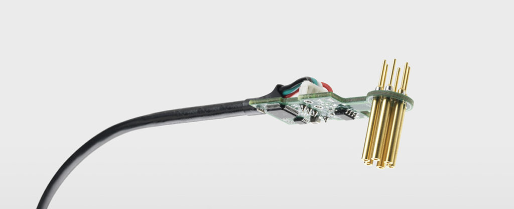
As mentioned elsewhere, it makes sense to consider a two-step overmolding approach in several situations:
- If the electronic assembly must be completely sealed
- If the positioning of the electronic package inside the final overmold is critical (sensor, antenna or Bluetooth chip locations may dictate accurate location)
- If the project requires light pipes, we will typically premold light pipes with semi-transparent amber and complete the overmold with opaque black material
- When overmold design has large variation in section thicknesses and sink in the final product is unacceptable
- When an assembly has wired components and wires must be fully contained in the overmold
There are a number of things to consider in a two-step overmolding approach. This article will only focus on the premold design itself.

Sealing
In most cases, it is necessary to use locator pins, shelves or other tooling features in order to hold a PCBA accurately within the moldset cavity. These features will leave holes to the PCB surface after molding. Such holes must be considered potential leak paths. With two-step overmolding we add molded locator features in premold. These features serve to locate the premolded assembly correctly in the overmold cavity. Any remaining holes to the PCB can then be sealed during the final molding operation.
This molding approach also allows the two molding steps to be performed with different molding materials. Oftentimes, the first step is molded with a material that offers strong adhesive properties. The second step may employ with a material that offers the right performance characteristics, such as solvent resistance, abrasion resistance or higher durometer. Seal and protect!
Positioning
Some assemblies can be overmolded in a single shot using a connector, or similar, to “hold” the assembly in the moldset cavity. The downside is that this approach will allow the electronic assembly to float inside the overmold cavity. This may be acceptable for a simple USB memory stick, but is not accurate enough for a sensing element or a transmitting device.
- Sensors with Hall Effect devices typically need to be very accurately located and only have a thin layer of molding material over the sensing IC.
- Optical sensors need a consistent layer covering them to measure light accurately.
- Board-mounted antennas typically need a consistent layer of overmold material to avoid any inconsistent signal loss.
- Bluetooth or RF transmitters must have a very consistent, thin layer of material covering them in order to function. Some cannot tolerate overmolding at all and will need a keep-out feature during the overmolding operation and will require a secondary operation to protect them.
The first molding step will ensure accurate location of any critical component. The second molding step will complete the overmolding process and seal the electronics.
SMT LED
It’s common for PCBAs to have surface mount LED indicator lights. Conventional, acrylic light pipes are not ideally suited for overmolding as the molding material might bleed into the light pipe and block the light from the LED. Cavist would normally recommend molding the light pipes in a clear premold material. This eliminates potential leak paths along an acrylic light pipe. Cavist will also use the light pipe to serve as a locating feature in the overmold cavity. Color separation between adjacent, different color LEDs is achieved by using blades in the premold tooling. The opaque overmold material will then isolate the individual light pipes in the second molding step.
Variation in molded section thickness : Surface quality.
A printed circuit board assembly may have some discrete tall components, but the final product is intended to have smooth, flat surfaces for a nice aesthetic look. If an assembly with significant variation in component heights is overmolded in a single shot, there will be sink in the finished product, as the molding materials will contract 1.5 to 2%. Adding a premold operation will help improve the cosmetics of an overmolded assembly quite dramatically. The premold should be designed as a slightly undersized version of the final shape, leaving an even skin thickness (1-2 mm) for the second shot. When designing the premold locator features, it is important to factor in material shrinkage. The locators will shrink as well, so they must be slightly oversized relative to the final overmold shape. If this premold is designed correctly, the end result is a really good surface quality!
Wire Management
Whenever a cable, or a bundle of wires, is terminated on a PCB, the overmolded product must be designed to prevent these wires from showing on the surface of the finished product. This can be done effectively with zip ties or crimps, but that can be time consuming, and the quality of “wire management” is only as good as the attention paid to the task. A premolding step guarantees that the wires are contained within the first molding step, irrespective of how long they are. They may be visible on the premolded assembly surface, but will be completely covered during the final overmolding step.
Two-step overmolding, as the name indicates, requires twice the molding time and labor. Certain products, however, demand this extra molding step, in order to meet the product design and/or aesthetic requirements.